
09-25: Abdelghani’s paper on NV sensing of edge magnetism in WS2 makes the cover of Advanced Functional Materials.

Check out articles in Phys.Org, AzoQuantum, Opli, Eurekalert, and others.
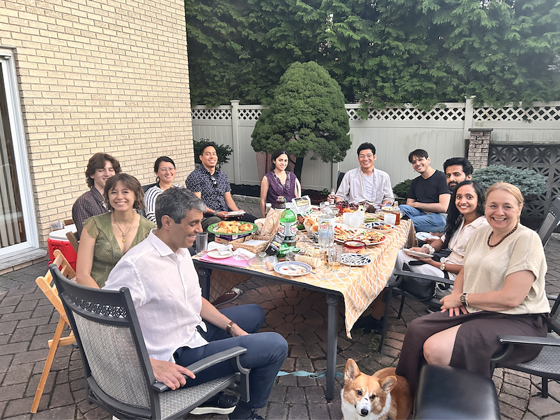
Featuring our newest group member, Tainee Maserati, bottom right.

See details of his presentation below:
Title: Progress in the Realization of Scalable Quantum Memory Nodes in 4H-SiC
Abstract: The vision of a global quantum internet is stalled by a fundamental obstacle in its core components, the quantum memory nodes (QMNs). Leading platforms face a debilitating trade-off: achieving the spectral tunability required for network-wide photon indistinguishability typically comes at the cost of degrading the emitter’s optical coherence and spin-to-photon interface. Resolving this challenge requires a new approach to deterministically control the quantum emitter’s environment.
In this talk, I will present our recent breakthrough in addressing this challenge by demonstrating precise electrical control over single silicon vacancy (VSi) centers in the industrial semiconductor 4H-Silicon Carbide. By embedding VSi centers within a p-i-n diode, we gain simultaneous control over two critical parameters. I will show that the applied electric field enables a wide-range DC Stark shift for deterministic spectral tuning. Crucially, we also demonstrate that the diode’s charge depletion mechanism actively suppresses spectral diffusion, leading to a significant narrowing of the optical linewidth towards the Fourier-transform limit. These results establish a robust, foundational method for engineering arrays of highly coherent and mutually indistinguishable quantum emitters. Finally, I will provide an outlook on how this powerful control technique can be integrated into nanophotonic waveguides, presenting a clear and viable pathway towards a novel hybrid QMN architecture designed to ultimately resolve the key scaling challenges in quantum networking.
This paper shows how a quantum emitter, the nitrogen-vacancy (NV) center in diamond, interacts in unexpected ways with a specially engineered photonic structure when moved around with a scanning tip. What has long been considered a drawback of the NV center—its broad and messy emission spectrum—turns out to enable a new type of coupling that reshapes its light in ways not seen before. This discovery has fundamental importance for quantum information technologies, since such coupling could help overcome long-standing challenges like spectral diffusion and open pathways toward robust spin–photon and spin–spin entanglement on a chip. At the same time, the work demonstrates a novel sensing capability: by analyzing the NV emission, we could reconstruct detailed, polarization-resolved images of the photonic modes with remarkable contrast. Beyond photonic structures, this polarization sensitivity could eventually be applied to detecting chiral molecules, which are central to biology and medicine. The paper is available online. See more here.
Here is the full reference:
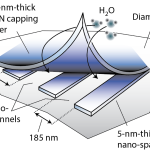
“Slow water in engineered nano-channels revealed by color-center-enabled sensing”, D. Pagliero, R. Khan, K. Elkaduwe, A. Bhardwaj, K. Xu, A. Wolcott, G. López, B. Radha, N. Giovambattista, C.A. Meriles, Nano Lett., published online in open access form. Also available as arXiv:2412.18969.
Learn more about this work here.